I recently bought a nRF51822 board to build a Bluetooth mouse for disabled people. The idea is that if I can get a Bluetooth HID service going on an nRF chip, then I can add various sensors to it and use it for their various needs. It can be a mouse, it can be a key or other things. I opted for the nRF family because they support open source applications and therefore a non-bloated development environment can be produced.
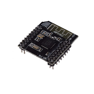
The board that I bought for the purpose is this:
 |
| nRF51822 board marked "HW-651". Note nothched corner. |
Well, there is a problem. No datasheet came with it nor can be found anywhere on the Internet. The pinout is completely unknown. It is also different from the pinouts of similar boards. So this post is to provide the information that I have found so far.
There are two pin headers marked "J1" and "J2", each with 2x9 pins. J1 is under the WiFi symbol, and J2 is under the marking "HW-651". Pin 1 has a square pad, and for J1 it is just next to the WiFi symbol and towards the outer edge of the board, and for J2 it is next to the "HW-651" marking, towards the center of the board. The pin numbers proceed in a zig-zag pattern as generally done in pin headers. BTW, the pin header is small and not the .1' type. It appears to be metric with 2mm spacing.
I traced the pinouts from the datasheet and a magnifying glass. The power supply pins and some others, were tested under the microscope with a continuity tester. A few of the pins are yet unidentified. They are marked "?" in the table.
This is J1 pinout:
| Func | Pin Hdr | IC Pin | IC Pin | Pin Hdr | Func |
|---|---|---|---|---|---|
| P0.21 | 1 | 40 | 13,33,34 | 2 | GND |
| P0.23 | 3 | 42 | 41 | 4 | P0.22 |
| P0.25 | 5 | 44 | 43 | 6 | P0.24 |
| ? | 7 | ? | ? | 8 | ? |
| P0.29 | 9 | 48 | 47 | 10 | P0.28 |
| P0.30 | 11 | 3 | 1,35,36 | 12 | Vdd |
| P0.00 | 13 | 4 | 13,33,34 | 14 | GND |
| P0.02 | 15 | 6 | 5 | 16 | P0.01 |
| P0.04 | 17 | 8 | 7 | 18 | P0.03 |
This is J2 pinout:
| Func | Pin Hdr | IC Pin | IC Pin | Pin Hdr | Func |
|---|---|---|---|---|---|
| P0.20 | 1 | 28 | 27 | 2 | P0.19 |
| P0.18 | 3 | 26 | 25 | 4 | P0.17 |
| SWCLK | 5 | 24 | 23 | 6 | SWDIO |
| P0.16 | 7 | 22 | 21 | 8 | P015 |
| P0.14 | 9 | 20 | 19 | 10 | P0.13 |
| P0.12 | 11 | 18 | 17 | 12 | P0.11 |
| P0.10 | 13 | 16 | 15 | 14 | P0.09 |
| P0.08 | 15 | 14 | 11 | 16 | P0.07 |
| P0.06 | 17 | 10 | 9 | 18 | P0.05 |
I will determine the missing pins under a microscope with continuity tester when I have more time. I have checked the pins VDD, GND, SWCLK, SWDIO to be correct (I got a reply from the chip with the progrmmer.)